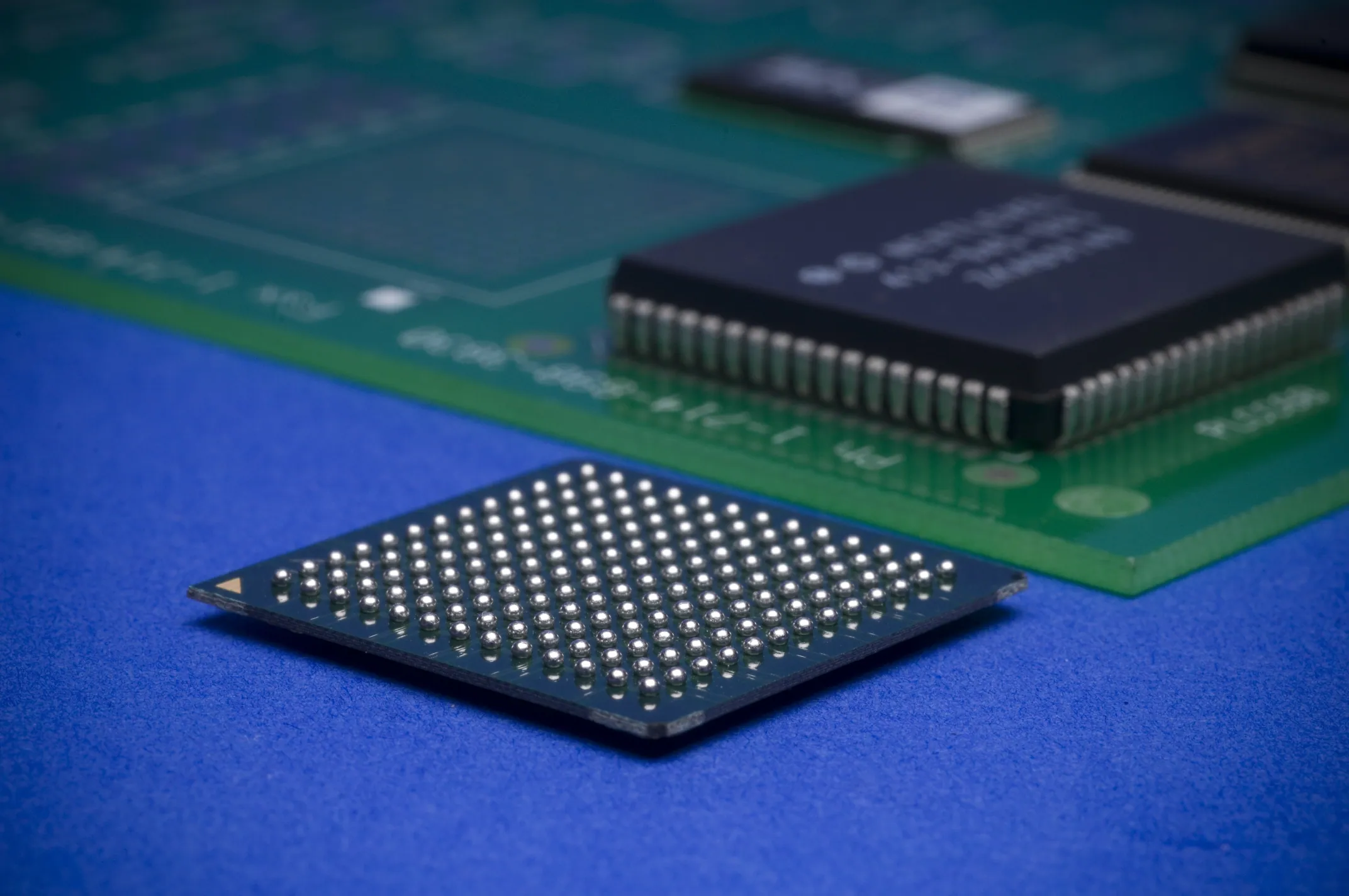
As the demand for smaller, faster, and more power-efficient electronics grows, the semiconductor industry continues to seek advanced solutions for connecting silicon dies to substrates. One such innovation is flip chip packaging, a method that allows the die to be mounted face-down directly onto the substrate using solder bumps. This approach offers significant advantages over traditional wire bonding by enabling higher I/O density, improved electrical performance, and better thermal management.
Unlike conventional IC packaging methods, where wires are used to connect the chip’s edges to the package, flip chip bonding provides a more direct electrical path. This reduces inductance and resistance, which is especially important in high-frequency or high-speed applications. Additionally, flip chip designs allow for more compact layouts, making them ideal for mobile devices, high-performance computing, and automotive electronics where space and performance are both at a premium.
Other common packaging types include wire bonding, chip-on-board (COB), and wafer-level packaging (WLP). While wire bonding remains cost-effective and reliable for many low-to-mid-range applications, it struggles with performance limitations in advanced systems. WLP and 2.5D/3D packaging offer higher integration and miniaturization, but often come with greater complexity and cost.
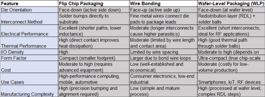
Here’s a table comparing flip chip packaging with wire bonding and wafer-level packaging (WLP) across several key parameters:


Overall, flip chip bonding and packaging present a compelling alternative for applications requiring high speed, efficient heat dissipation, and compact design. As technology continues to evolve, flip chip solutions are likely to play an increasingly important role in the future of semiconductor packaging.