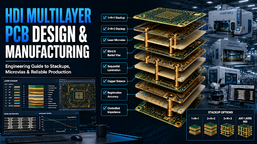
As electronic devices continue to become smaller, faster, and more complex, printed circuit boards must accommodate higher component density without compromising electrical performance or reliability. High Density Interconnect technology has become a practical solution for achieving these goals, particularly in industries such as telecommunications, automotive electronics, industrial automation, aerospace, and medical devices.
Designing an HDI multilayer PCB requires more than selecting a stackup with additional routing layers. Engineers must carefully consider build up structures, microvia configuration, sequential lamination, copper balance, material selection, and manufacturing tolerances to ensure the design can be fabricated consistently.
This guide explores the key engineering and manufacturing considerations involved in HDI multilayer PCB production, helping designers make informed decisions that improve manufacturability, reliability, and long term product performance.
Understanding HDI Multilayer PCB Structures
Unlike conventional multilayer PCBs, HDI boards use laser drilled microvias and sequential build up layers to increase routing density while maintaining compact board dimensions.
The choice of stackup depends on routing complexity, signal integrity requirements, component density, and manufacturing cost.
Common HDI structures include:
1+N+1
One build up layer is added to each side of the core.
This is one of the most common HDI configurations and is suitable for products with moderate routing density. It provides additional routing channels while maintaining relatively simple manufacturing processes.
Typical applications include:
- Industrial control systems
- Consumer electronics
- Communication modules
- Embedded computing devices
2+N+2
Two sequential build up layers are added on each side of the core.
Compared with 1+N+1, this configuration provides significantly greater routing flexibility for high pin count components such as modern processors and memory devices.
Typical applications include:
- Networking equipment
- Automotive control units
- High speed communication systems
- Medical imaging equipment
3+N+3
Three build up layers are added on each side of the core.
This architecture supports extremely dense routing while increasing manufacturing complexity through additional lamination cycles.
Designers typically choose this structure for products requiring advanced interconnection density without substantially increasing PCB size.
Any Layer HDI
Any Layer HDI allows laser microvias between nearly every adjacent layer.
Instead of routing through a central core using conventional through holes, designers gain much greater routing flexibility throughout the entire stackup.
Although Any Layer designs can significantly improve routing efficiency, they also require advanced manufacturing capability, strict process control, and comprehensive inspection.
Selecting the Appropriate Build Up Architecture
Choosing the correct HDI architecture involves balancing electrical performance, manufacturing complexity, and project cost.
Questions engineers should evaluate include:
- How many high pin count components require breakout routing?
- Are fine pitch BGAs being used?
- How many differential signal pairs must be routed?
- What board thickness limitations exist?
- Is future product expansion expected?
Selecting a more complex stackup than necessary may increase fabrication cost without delivering measurable design benefits.
Conversely, choosing an overly simple structure may create routing congestion that complicates later design revisions.
Close collaboration between design engineers and manufacturing teams during stackup planning often leads to more efficient solutions.
Stacked vs Staggered Microvias
One of the most important design decisions in HDI fabrication involves selecting the appropriate microvia structure.
Stacked Microvias
Stacked microvias are positioned directly above one another, creating a vertical electrical connection through multiple build up layers.
Advantages include:
- Reduced routing distance
- Higher routing density
- Improved component breakout
- Compact PCB layouts
However, stacked microvias require precise copper filling and careful process control during fabrication. Poorly filled vias or plating defects can reduce long term reliability.
Staggered Microvias
Staggered microvias are offset between adjacent layers rather than being aligned vertically.
Benefits include:
- Lower manufacturing complexity
- Reduced mechanical stress
- Improved fabrication yield
- Lower production cost
Because each via terminates in a different location, stress is distributed more evenly during thermal cycling.
The choice between stacked and staggered structures depends on routing density, available board area, reliability requirements, and manufacturing capability.
Sequential Lamination and Build Up Cycles
Every additional build up layer requires another sequential lamination cycle.
Each cycle introduces new manufacturing challenges, including:
- Layer registration
- Resin flow control
- Material expansion
- Copper alignment
- Drilling accuracy
As build up cycles increase, maintaining dimensional stability becomes increasingly important.
Manufacturers use carefully controlled lamination parameters and inspection procedures to minimise cumulative alignment errors throughout the fabrication process.
Designers should recognise that more lamination cycles generally increase fabrication time, inspection requirements, and manufacturing complexity.
Copper Balance and Signal Integrity
Copper distribution has a significant influence on both manufacturability and electrical performance.
Uneven copper density may contribute to:
- Board warpage
- Lamination stress
- Uneven plating
- Registration variation
- Thermal imbalance
Maintaining balanced copper distribution across the PCB helps improve dimensional stability throughout manufacturing.
From an electrical perspective, consistent copper geometry also supports controlled impedance routing and reduces signal integrity problems in high speed digital designs.
Engineers should review copper balance during layout rather than relying on manufacturing adjustments later in production.
Registration Accuracy Across Multiple Layers
As HDI stackups become more complex, registration accuracy becomes increasingly critical.
Small alignment errors may affect:
- Microvia positioning
- Fine line routing
- Annular rings
- BGA breakout regions
- Controlled impedance structures
To minimise these risks, manufacturers monitor registration throughout fabrication using methods such as:
- Automated Optical Inspection
- X ray alignment verification
- Cross section analysis
- Statistical process control
Accurate registration becomes particularly important for designs incorporating multiple sequential lamination cycles and laser drilled microvias.
Material Selection for HDI Multilayer Boards
The performance of an HDI multilayer PCB depends not only on its layer structure but also on selecting materials that match the electrical, thermal, and mechanical requirements of the application.
Several factors should be considered during material selection, including:
- Dielectric constant for signal integrity
- Loss characteristics for high frequency applications
- Glass transition temperature
- Thermal expansion
- Moisture absorption
- Mechanical stability during sequential lamination
Selecting compatible materials early in the design process helps reduce manufacturing risks and supports more predictable electrical performance throughout the product’s service life.
For projects requiring controlled impedance, material properties should be reviewed alongside stackup planning rather than after PCB layout has been completed.
Reliability Considerations During HDI Manufacturing
As routing density increases, maintaining long term reliability becomes increasingly important.
Each additional build up layer, laser drilled microvia, and lamination cycle introduces manufacturing variables that must be carefully controlled.
Reliable HDI production depends on factors such as:
- Consistent copper plating
- Accurate resin flow
- Stable layer registration
- Proper microvia filling
- Controlled drilling parameters
- Material compatibility
Manufacturers typically validate these processes through inspection and process monitoring to identify potential issues before boards enter assembly.
Design decisions that simplify fabrication often improve manufacturing yield while reducing the likelihood of defects developing during long term operation.
Design for Manufacturability Best Practices
Many fabrication challenges can be avoided by considering manufacturing limitations during PCB layout instead of waiting until production begins.
Design for Manufacturability (DFM) reviews allow engineers and manufacturers to evaluate the design before fabrication starts.
Common DFM considerations include:
- Stackup optimisation
- Microvia placement
- Trace width and spacing
- Copper balancing
- Drill sizes
- Pad dimensions
- Controlled impedance routing
- Panel utilisation
Early collaboration between the design team and the manufacturer often reduces engineering revisions, shortens development schedules, and improves production efficiency.
Inspection and Verification Throughout Production
Inspection is essential throughout HDI manufacturing because defects can become increasingly difficult to detect after additional build up layers are laminated.
Rather than relying only on final inspection, manufacturers typically perform verification at multiple production stages.
Common inspection methods include:
- Automated Optical Inspection
- X ray inspection
- Cross section analysis
- Electrical testing
- Dimensional measurement
- Surface finish verification
These inspections help confirm that manufacturing processes remain within specification while identifying potential issues before they affect later production stages.
Comparing Common HDI Architectures
Selecting the most appropriate HDI structure requires balancing routing density, manufacturing complexity, and project requirements.
| HDI Structure | Typical Routing Density | Manufacturing Complexity | Typical Applications |
| 1+N+1 | Moderate | Lower | Industrial controls, consumer electronics |
| 2+N+2 | High | Moderate | Automotive electronics, networking equipment |
| 3+N+3 | Very High | High | Advanced computing, aerospace, medical systems |
| Any Layer | Maximum | Highest | Ultra compact, high performance electronic products |
Rather than selecting the most advanced structure by default, engineers should choose the architecture that satisfies routing requirements while remaining practical to manufacture.
Working with an Experienced Manufacturing Partner
Even an excellent PCB layout benefits from collaboration with a knowledgeable manufacturing team.
An experienced HDI PCB manufacturer can provide valuable feedback on stackup design, sequential lamination planning, copper balancing, manufacturability, and inspection strategies before fabrication begins.
Topics worth discussing during the engineering review include:
- Build up architecture
- Microvia configuration
- Material selection
- Controlled impedance requirements
- Registration tolerances
- Inspection plans
- Prototype objectives
- Production scalability
Addressing these considerations before production reduces the likelihood of engineering changes and helps improve manufacturing consistency.
Common Design Mistakes to Avoid
Several design practices can increase fabrication complexity or reduce production yield if they are not addressed early.
Common mistakes include:
- Selecting unnecessarily complex stackups
- Using stacked microvias where staggered structures would be sufficient
- Ignoring copper balance during layout
- Delaying impedance planning until after routing
- Overlooking material compatibility
- Failing to consider sequential lamination requirements
- Neglecting Design for Manufacturability review
Avoiding these issues helps simplify fabrication while improving both reliability and manufacturing efficiency.
Key Design Evaluation Checklist
Before releasing an HDI multilayer PCB for fabrication, engineering teams should confirm that the following items have been reviewed.
| Design Area | Verification |
| Stackup architecture | Selected according to routing requirements |
| Build up layers | Appropriate for component density |
| Microvia structure | Stacked or staggered selected appropriately |
| Copper balance | Even distribution across all layers |
| Controlled impedance | Verified through stackup planning |
| Material selection | Suitable for electrical and thermal requirements |
| Registration | Manufacturing tolerances reviewed |
| DFM review | Completed before fabrication release |
Using a structured checklist helps identify potential manufacturing challenges before they become costly production issues.
Final Thoughts
Designing an HDI multilayer PCB requires balancing electrical performance, routing density, manufacturing capability, and long term reliability. Decisions involving stackup architecture, sequential lamination, microvia configuration, copper balance, and material selection all influence how successfully a design can transition from engineering to production.
While advanced structures such as 2+N+2, 3+N+3, and Any Layer HDI provide greater routing flexibility, they also require tighter process control and more comprehensive inspection throughout fabrication. Selecting the appropriate architecture should always be based on project requirements rather than maximum capability alone.
Working closely with manufacturing specialists during the design stage helps identify potential fabrication challenges early and supports a smoother transition into production. By combining thoughtful engineering with thorough Design for Manufacturability review and robust quality control, development teams can improve production yield, reduce revisions, and enhance the long term reliability of HDI multilayer PCB assemblies.